-
Viewpoint on 'IONS'
Viewpoint on 'Scientific Literacy'
- Proudly sponsored by
-


-
A Brighter Summer under the Ice

While Venice and other coastal cities around the world are slowly sinking, during the Arctic summer the waters underneath the ice become brighter and brighter. Are these two scenarios connected to the continuous thinning of Arctic ice?
-
What a Molecular Transistor!
How far can a single, tiny molecule go? Exceeding most people's imagination, researchers have shown that a single molecule can actually work as a transistor for photons.
-
Forensic Optics: Transforming a Hair into a Travel Log
Solving crimes requires and complicated investigations in order to find clear evidence. Now, it is possible to obtain information about a suspect's travel history by analyzing their hair.
THE VIEWPOINT by Banqiu Wu & Ajay Kumar
Extreme Ultraviolet Lithography:
Towards the Next Generation of Integrated Circuits
Lithography is the most challenging technology in the semiconductor industry. The most promising next generation lithography technology is extreme ultraviolet lithography (EUVL). EUVL was proposed long ago, in 1988, but its implementation has been postponed several times. Presently, most "showstoppers" are gone, but there are still several challenges that need to be addressed. The semiconductor industry is now getting ready to use EUVL in a pre-production phase, and EUVL might be implemented for 32 nm and 22 nm technological nodes. High volume manufacturing EUVL printers will be delivered to multiple end-users from 2010.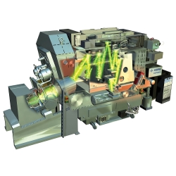
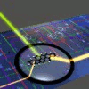
ASML Alpha Demo Tool. The sketch represents a developmental full-field EUVL scanner recently developed by ASML. The UV light source (based on a discharge-produced plasma DPP) is placed on the left. The generated UV light is directed by a series of Bragg mirrors to the reflective mask used to pattern the resist (on the right). The entire tool is kept in vacuum conditions to prevent the absorption of the UV light by the air.
A brief history
Nearly all of today's electronic devices rely on key internal semiconductor components, known as integrated circuits (ICs). ICs are manufactured through a critical process known as lithography, which is the determining factor in keeping pace with the quest of the electronics industry to shrink ICs and other related products even more.Lithography is a patterning method that creates an IC layout on a resist layer of a silicon wafer or other semiconducting substrate. It mainly consists of three parts: a) the pattern printer, b) photoresist technology, and c) the mask fabrication.
Lithography technology was introduced to the semiconductor industry when ICs were invented in 1958. The original lithography used light of the visible g-line (436 nm) and the ultraviolet i-line (365 nm), which was easily produced with a mercury arc lamp. With the progress of technology and the reduction of the feature size, the wavelength of the exposure light had to be reduced several times. When the IC feature size was reduced to about half a micron (500 nm), the g-line and the i-line could no longer be used, and therefore deep ultraviolet 248 nm KrF and 193 nm ArF excimer lasers were introduced. Currently, the 193 nm lithography combined with immersion and double patterning technology is the state of the art.
Shorter wavelength lithography, known as next generation lithography (NGL), has been studied in order to produce IC with even smaller features. NGL uses shorter ultraviolet light (157 nm), extreme ultraviolet (EUV) light (e.g. 13.5 nm), X-ray (0.4 nm), and the even shorter wavelengths of electron and ion beams. Back in 1988 a technology named soft X-ray projection lithography was proposed. However, since the wavelength range of EUV and soft X-ray is not sharply defined (the former lays approximately between 50 nm and 5 nm, and the latter between 5 nm and 0.2 nm), this technology in 1994 came to be known worldwide as EUVL.
Compared with other NGL methods — e.g. proximity X-ray lithography (PXL), electron projection lithography (EPL), and ion projection lithography (IPL) — EUVL is a relatively new member of the NGL league. Due to its remarkable optical convenience — it is accepted as the natural extension of optical lithography — the development of EUVL technology has been relatively fast and since 1999 it has been the most promising NGL technology.
To this day, research and development of EUV technology has cost several billion US dollars worldwide. In order to understand this, we must keep in mind that a single EUV exposure tool is very costly, e.g. about US$ 70 million. This can only be supported because global lithography production itself is a large-scale industry, measured on an annual revenue basis of several billion US dollars.
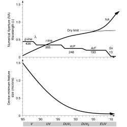
The Moore Law of lithography. The constant downsizing of the wavelength used in lithography and the increase in the numerical aperture (NA) have permitted the continuous reduction of the minimum integrated circuit feature size. The shift from 193 nm to 13.5 nm is the greatest jump the industry has experienced so far. Adapted with permission from "Extreme Ultraviolet Lithography," McGraw-Hill Professional, 2009.
One important aspect to bear in mind is the fact that all available materials are strong absorbers of EUV light and no material is transparent enough to make use of refractive optics (e.g. lenses). Therefore, it is necessary to make use of reflective optics only (e.g. mirrors) in EUVL optical systems. EUV light is reflected on multi-layer mirrors, known as Bragg-reflectors, usually consisting of molybdenum and silicon (Mo/Si) multilayer. As a matter of fact, the availability of suitable mirrors has determined the choice of the wavelength used in EUVL. Despite the broad range of EUV wavelengths, the most commonly used are the ones that lie between 11.3 nm and 11.6 nm (for which Mo/Be multilayer reflective mirrors are available) and the ones between 13.3 nm and 13.6 nm (for which Mo/Si multilayer reflective mirrors can be used). To date, the Mo/Si multilayer for 13.5 nm EUV is the leading candidate. Theoretically, the thickness of a pair of layers should be about half the wavelength: for 13.5 nm EUV light, the Mo/Si thickness is approximately 6.75 nm (e.g., Mo 2.7 nm and Si 4.1 nm); for 11.4 nm EUV, Mo/Be thickness is 5.7 nm (Mo 2.3 nm and Be 3.4 nm).
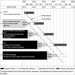
2007 ITRS lithography roadmap for semiconductors. At the moment, it is predicted that EUVL will have some pilot-scale applications at the 32 nm technology node or will be used in full production for the 22 nm half-pitch technology node. High volume manufacturing (HVM) pre-production (beta) exposure aligners will be delivered to multiple end-users starting in 2010. Adapted with permission from "Extreme Ultraviolet Lithography," McGraw-Hill Professional, 2009.
The map of worldwide research
Since 1988, many studies on EUVL have been conducted in North America, Europe, and Asia, through state sponsored programs, industrial consortiums, and individual companies.In the early and mid-1990s, systematic research was mainly performed by the Lawrence Livermore National Laboratory (LLNL), Sandia National Laboratory (SNL), and Lawrence Berkeley National Laboratory (LBNL), as well as AT&T Bell Laboratories and several universities. In 1997, an industrial consortium, the EUV LLC, was formed by Intel, Motorola, and Advanced Micro Device (AMD), to continue work on EUVL. At the same time, the Virtual National Laboratories (VNL) was also formed by LLNL, SNL, and LBNL to conduct a program sponsored by EUV LLC.
In Europe, an industrial consortium, the Extreme Ultraviolet Concept Lithography Development System (EUCLIDES), was formed in 1998 by ASM Lithography (ASML), Carl Zeiss, and Oxford Instruments. Since then, EUVL studies in Europe have made significant progress, with ASML leading.
In Japan, original studies in EUVL were performed in NTT LSI Laboratories, and publications were found dating from 1989. Other EUVL pioneer work was carried out by Nikon and Hitachi around 1990. The Association of Super-Advanced Electronics Technologies (ASET) was established in 1996, launching its EUVL program in 1998. The Extreme Ultraviolet Lithography System Development Association (EUVA) was established in 2002.
Today, EUVL studies are conducted mainly by industrial consortiums and companies, including SEMATECH in US, IMEC in Europe, Selete in Japan, as well as Globalfoundry, Intel, Samsung, TSMC, Toshiba, Hynix, and IBM.
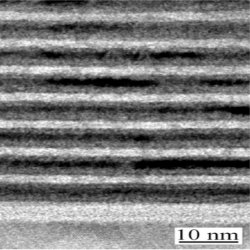
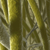
Section of a Bragg Mirror for EUVL. Transmission electron microscope (TEM) image of a Mo/Si multilayer cross section. Such materials are employed to produce Bragg mirrors that reflect EUV light.
The challenges
To date, no "showstoppers" have been identified, but challenges are present in almost every aspect of EUVL technology. Some challenges are common to all NGL technologies, e.g. resist resolution and line-edge roughness (LER). Other challenges are unique to EUVL, e.g. resist outgassing owing to the EUVL high-vacuum environment. In the past 20 years the main topics of research in EUVL have been: source, optics, mask, multilayer coating, resist, metrology, reticle handling, defects, and contamination control.Today, commercial alpha lithography step-and-scan tools are installed with full field capability; EUVL power at intermediate focus (IF), however, has not yet met the target of 180 watt intermediate focus (IF) power required for volume manufacturing. EUV IF power has been improving gradually from xenon to tin discharge-produced plasma (DPP), or to laser-produced plasma (LPP). The current EUV source can only supply approximately 50 watts. Recent progress on the LPP EUV source shows a very promising result, since it is expected to reach 100 watts by the end of 2009. Collector and projection optics meet all specifications except for flare control. The extremely high temperature EUV source plasma may mean a short lifespan and the degradation of the condenser.
EUVL resist technology development is dependent on the development of the exposure tools. Once the small field exposure tools became available, significant progress was made in developing EUVL resists. To date, a 1:1 line-and-space line resolution of around 20 nm has been obtained on CAR, which removes the "showstopper" in implementing EUVL. The resist absorption of EUV and the effects on the resist profile are also challenging. Sensitivity and LER also need improvement. EUV source power also affects resist technology. Higher EUV source power will reduce the pressure on resist sensitivity. The critical challenge is to meet requirements on resist resolution, sensitivity, and LER simultaneously.
It is a critical task to create a defect-free EUVL mask. EUVL mask technology includes mask blank preparation and pattern fabrication, as well as the use of non-pellicle masks. This may be the most challenging aspect of this new technology, but it is still a workable one. In fact, although EUVL masks require a complicated multilayer, a capping layer, a buffer, and an absorber, they are relatively easy to fabricate compared with other NGLs that use membrane masks. EUVL mask pattern generation and transfer face issues similar to those for other NGLs. Pattern transfer fidelity is also a challenge. For non-pellicle masks, movable pellicles and thermophoretic protectiona were proposed. More progress is necessary, however, for this technology to be deemed practical.
The adoption of EUVL will also be influenced by the extension of the modern optical lithography (e.g. the 193 nm immersion lithography, combined with double patterning techniques). The cost of ownership will also be a critical consideration in the adoption of EUVL.
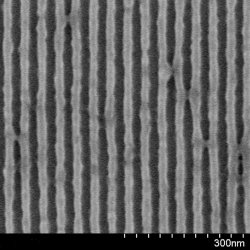
EUVL at work. Scanning electron microscope (SEM) image of a 22-nm half-pitch line-and-space pattern printed using EUVL.
The opportunities
EUVL was originally planned in 1988 for the 100 nm technology node. However, the extension of optical lithography delayed the adoption of EUVL and other NGL technologies. In 1997, implementation was predicted for the 65 nm node. A further extension of optical lithography reduced the predicted EUVL implementation to under the 45 nm node. The immersion exposure technology combined with the double patterning method delayed EUVL implementation further. At the moment it is predicted that EUVL will have some pilot-scale applications at the 32 nm technology node or will be used in full production for the 22 nm half-pitch technology node.EUVL implementation has been repeatedly delayed; optical lithography, on the other hand, has its inherent limit in resolution (R) and depth of focus (DOF), as shown by the following two equations:
R = k1 λ / NA (Eq. 1)
DOF = k2 λ / NA2 (Eq. 2)
where λ is the wavelength, NA the numerical aperture, and where k1 and k2 are constants. Optical lithography has been pushed to the limit using immersion exposure technology and high NA, which allow for a great improvement on the resolution. At the state of the art, the NA is as high as 1.35, and may increase to about 1.70 for the 32 nm node technology. On the other hand, high NA values significantly decrease the depth of focus and make operation more difficult.
| NA 0.25 | NA 0.35 | NA 0.50 | |
| Node 32 nm | 0.59 | 0.83 | 1.19 |
| Node 22 nm | 0.41 | 0.57 | 0.81 |
| Node 16 nm | 0.30 | 0.41 | 0.59 |
| Node 11 nm | 0.20 | 0.29 | 0.41 |
EUVL was introduced as a high k1 (see Eq. 1) technology, thus it offers potential extendibility to smaller feature size nodes (see Table). For a conservative k1 of 0.40 and 0.25 NA, the resolution based on Eq. 1 can reach 22 nm half pitch features. 10 nm half pitch features can be printed when using an aggressive optical design with 0.45 NA and a k1 of 0.32. This possibility gives EUVL a significant resolution advantage, compared with 193 nm optical lithography.
Outlook
In the last two decades EUVL has been the subject of intense research activity. Many technological challenges have been overcome and it is now agreed that there is no "showstopper" for EUVL technology; nevertheless, before its implementation is deemed practical, many critical challenges must be addressed. This being the case, only cautious optimism is called for with regard to imminent EUVL applications.Adoption time mainly depends on investment in research and development, driven by the extension limits of current optical lithography. In fact, with high NA and resolution enhancement techniques (RET) on EUV lithography, it is quite possible to push EUVL further down still, to another technology node. Based on this prediction, a two-generation node lithography technology will be strongly competitive.
EUVL has not only been a hot topic recently, but it also led to heavy industrial investment and practice. High volume manufacturing (HVM) pre-production exposure aligners will be delivered to multiple end-users starting in 2010. This intensive investment seems to signify that EUVL is bound to be imminent.
Banqiu Wu & Ajay Kumar
2009 © Optics & Photonics Focus
Banqiu Wu, Ph.D. is a Distinguished Member of the Technical Staff and the CTO of the Mask Etch and Clean Division, Applied Materials, Inc. Dr. Wu has 20 years of experience in plasma, etching, mask, lithography, and advanced materials. He has published over 50 articles, holds multiple patents, and authored and co-authored several books.
Ajay Kumar, Ph.D. is the General Manager of the Cleans and Mask Products Business Group, Applied Materials, Inc. Dr. Kumar received a Ph.D. from Indian Institute of Technology in Applied Physics and an MBA from Santa Clara University. He holds more than 100 US Patents and has published more than 75 technical papers.